


All Products
-
 Tyler MartinThe quality of the PCBs I received from this company was outstanding. They were well-made and exceeded my expectations.
 -
Olivia AndersonI've been using this company for all of our company PCB needs for years and I have never been disappointed. Their products are always consistent and reliable, and their prices are very competitive.
-
Ashley Williamswell-packaged and arrived in perfect condition. I would definitely recommend them to anyone in need of high-quality PCBs
Contact Person :
Xu
Phone Number :
0086 18565798250
Whatsapp :
+008618576405228
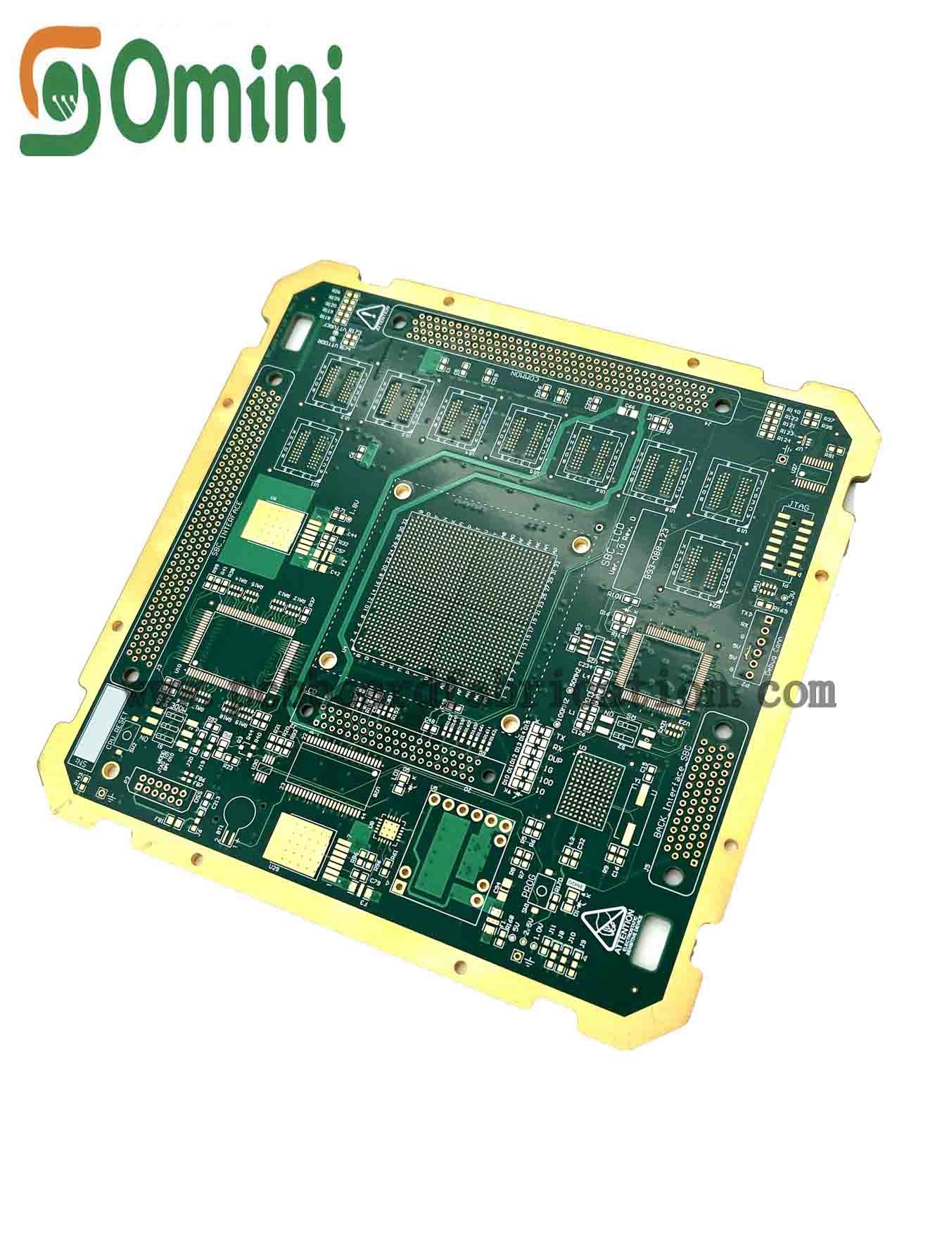
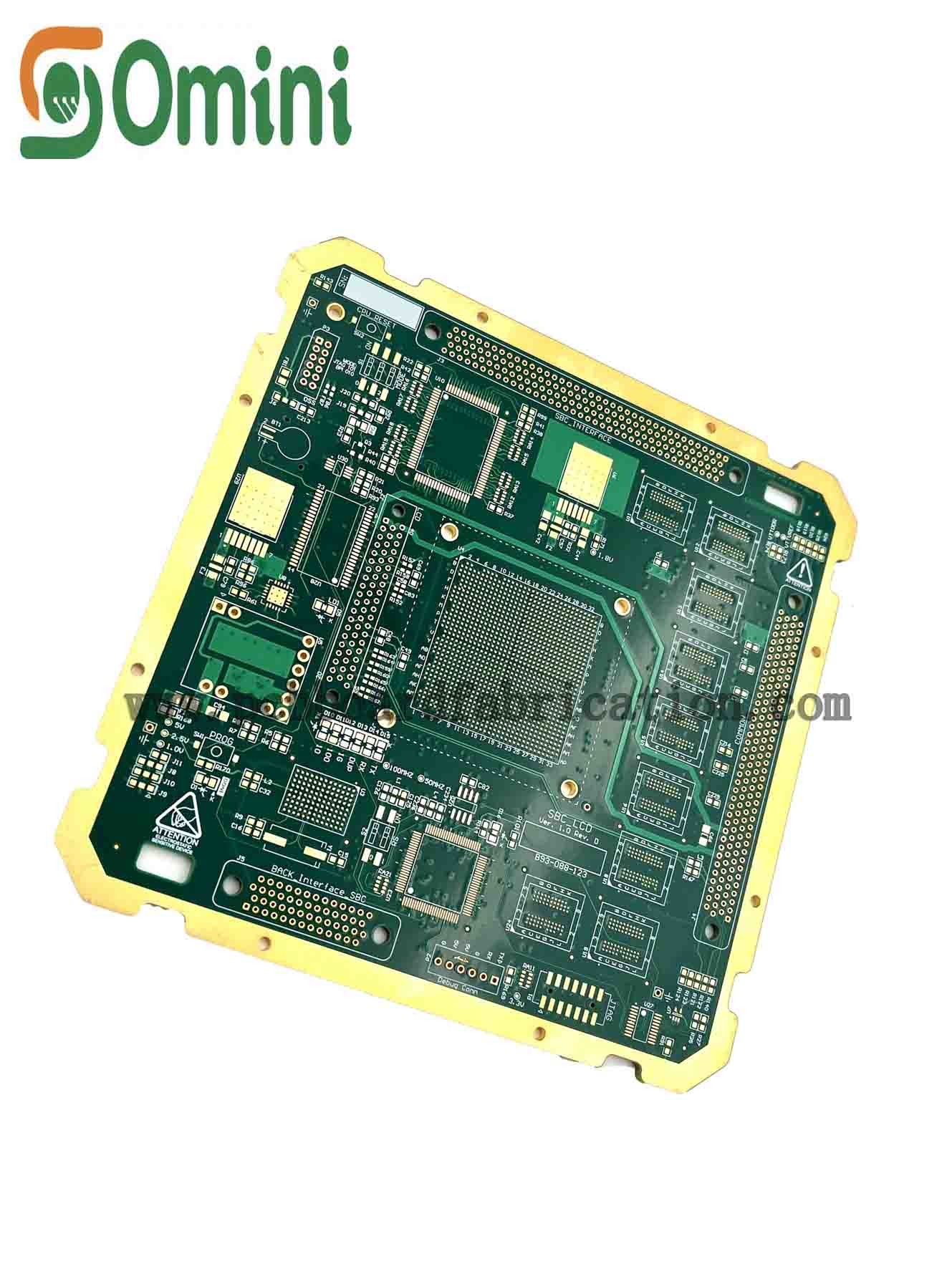
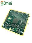
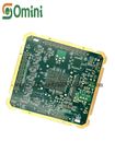
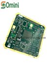
Computer Demand 0.2mm 8Mil BGA PCB Multilayer Printed Circuit Board

| Place of Origin | ShenZhen |
|---|---|
| Brand Name | Omini |
| Certification | ISO9001,UL,REACH |
| Model Number | Omini-01003 |
| Minimum Order Quantity | Negotiate |
| Price | Negotiate |
| Packaging Details | Vacuum packaging+Foam cotton+Carton +Strap |
| Delivery Time | 3-8 working days |
| Payment Terms | T/T, Western Union, MoneyGram,L/C, paypal |
| Supply Ability | 9,999,999 |

Contact me for free samples and coupons.
Whatsapp:0086 18588475571
Wechat: 0086 18588475571
Skype: sales10@aixton.com
If you have any concern, we provide 24-hour online help.
xProduct Details
| Material | TG170 FR4 | Board Thickness | 1.6mm |
|---|---|---|---|
| Copper Thickness | 2 OZ | Min. Line Width | 3mil |
| Min. Hole Size | 3mil | Layer | 10 Layer |
| Surface Finish | ENIG | Application | Computer Demand |
| High Light | 8mil BGA PCB,0.2mm Multilayer Printed Circuit Board,8Mil Multilayer Printed Circuit Board |
||
Product Description
Quick details:
Base Material: Shengyi S1000-2M
Copper Thickness: 2 oz
Board Thickness: 1.6 mm
Min. Hole Size: 0.2mm
Min. Line Width: 3 mil
Min. Line Spacing: 3 mil
Surface Finishing: ENIG
Board Size: Customize
Application:Computer Demand
IPC Degree: IPC Class 2
Maximum board width: Customize
Type: Multilayer PCB
Certificate: TS16949.ISO14001.ROHS. ISO9001
Color: Green
Package: Vacuum packing
Description of BGA Multilayer Printed Circuit Board
BGA stands for "Ball Grid Array," and PCB stands for "Printed Circuit Board." A BGA multilayer PCB is a type of printed circuit board that is designed to accommodate BGA components.
A BGA component is a type of surface-mounted device that uses an array of small solder balls to connect it to the PCB. BGA components are used in electronic devices where space is at a premium, and high-speed data transfer is required.
A multilayer PCB is a printed circuit board that has multiple layers of conductive material sandwiched between insulating layers. The use of multiple layers allows for a more complex circuit to be designed, while still maintaining a small form factor.
When designing a BGA multilayer PCB, careful consideration must be given to the placement of the BGA components, as well as the routing of the traces between the layers. This is because the small size of the solder balls used to connect the BGA components to the PCB means that any errors in placement or routing can lead to a faulty or non-functional device.
Features of BGA multilayer PCBs
1.High component density: BGA components are used in electronic devices where space is at a premium, and multilayer PCBs allow for more components to be packed into a smaller space.
2. High-speed data transfer: BGA components are used in devices where high-speed data transfer is required, and multilayer PCBs allow for complex signal routing to be done, minimizing the risk of signal interference.
3. Reduced noise: Multilayer PCBs have the advantage of being able to add power and ground planes between the signal layers, reducing electromagnetic interference and noise.
4. Increased reliability: The use of multiple layers in a PCB provides greater reliability by providing redundancy in the circuitry. In case of a break in one layer, the other layers can still provide a functional circuit.
5. Complex circuit designs: Multilayer PCBs allow for complex circuit designs to be implemented, with greater flexibility in terms of routing and layer stacking.
6. Thermal dissipation: BGA components generate heat, and multilayer PCBs can include additional copper layers for improved heat dissipation, reducing the risk of component failure due to overheating.
Specification of Omini Multi - layer Printed Circuit Board
| Layer | 2-24 layer |
| Material |
FR-4 Standard Tg 150℃, FR4-HighTg170℃, FR4- High Tg180℃, FR4- Halogen- free, FR4- Halogen- Free&High-Tg |
| Board thickness | 0.4mm-5.0mm |
| Board side | Min 6*6mm Max 600*700mm |
| Min.drilled hole size | 0.25mm |
| Min.line width | 0.075mm(3mil) |
| Min.line spaceing | 0.075mm(3mil) |
| Surface finish/treatment | Electroless/immersion gold/ENIG/Immersion silver/Organic solderability |
| Copper thickness | 0.5 oz - 2.0oz |
| Solder mask color | green/black/white/red/blue/yellow |
| Inner packing | Vacuum packing, Plastic bag |
| Outer packing | Standard carton packing |
| Hole tolerance | PTH:±0.076, NTPH:±0.05 |
| Certificate | UL, ISO9001, ISO14001, RoHS, CQC |
| Profiling Punching | Routing, V-CUT, Beveling |
| Assembly Service | Providing OEM service to all sorts of printed circuit board assembly |
![]()
![]()
![]()
![]()
![]()
![]()
FAQ:
Q1:Does Omini have enough capacity to prodece high-quality products?
A: Omini has 20 years of history in manufacturing PCB, more than 200 employees and 10,000㎡ factory area.We got the UL, ISO9001 certificates, and our production is sold abroad. We have engouh machines & equipment to ensure the quality, please check our Production Equipment list picturers.
Q2:How long does customers need to wait for the quotation and lead time?
A: We have a prefessional group to deal with your inquiry. In our working time, we will reply to your email within 30 minutes to show we have received your inquiry, Then we will send you our quotation in no more than 6 hours. Please noticed our working time is Monday to Friday, 8am to 24pm.
Q3:How can I make sure my PCB gerber is safety?
A: We promise we won't divulge your gerber to the 3rd party, one of our responsibilities is protecting customer information privacy and security, customer information can be included: company name, address, number, trademark, ect. And we could sign NDA with client if necessary.
Recommended Products