


All Products
-
 Tyler MartinThe quality of the PCBs I received from this company was outstanding. They were well-made and exceeded my expectations.
 -
Olivia AndersonI've been using this company for all of our company PCB needs for years and I have never been disappointed. Their products are always consistent and reliable, and their prices are very competitive.
-
Ashley Williamswell-packaged and arrived in perfect condition. I would definitely recommend them to anyone in need of high-quality PCBs
Contact Person :
Xu
Phone Number :
0086 18565798250
Whatsapp :
+008618576405228
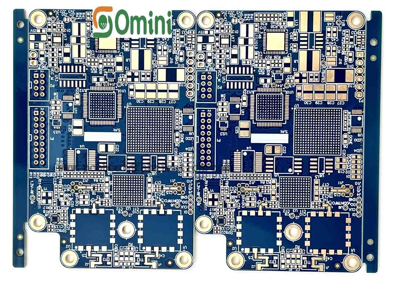
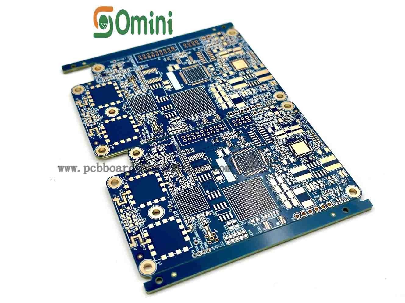
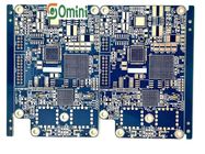
12 Layers 3 Order Communication PCB HDI Multilayer PCB Immersion Gold

| Place of Origin | China |
|---|---|
| Brand Name | Omini |
| Certification | ISO9001, ISO16949, ROHS |
| Model Number | PCB-0021 |
| Minimum Order Quantity | 1PCS |
| Price | Negotiate |
| Packaging Details | Vacuum packaging+foam cotton+carton+strap+ humidity card+Solder sample |
| Delivery Time | 3-8 working days |
| Payment Terms | T/T Paypal |
| Supply Ability | 30,000 square meter/month |

Contact me for free samples and coupons.
Whatsapp:0086 18588475571
Wechat: 0086 18588475571
Skype: sales10@aixton.com
If you have any concern, we provide 24-hour online help.
xProduct Details
| Product Name | 12 Layers 3 Order HDI Communication PCB | Base Material | TU872slk |
|---|---|---|---|
| Copper Thickness | 0.5OZ | Min Hole | 2.5mil/2.5mil |
| Board Thickness | 1.2mm | Layers | 3+6+3 HDI PCB |
| Application | Communication Product Pcb Board | ||
| High Light | 3 order HDI Communication PCB,HDI Multilayer PCB Immersion Gold,12 Layers HDI Multilayer PCB |
||
Product Description
12 layers 3 order HDI Communication PCB
Quick details:
Model : 12 layers 3 order HDI Communication PCB
Layers : 12Layers
Material : TU872slk
Construction : 3+6+3 HDI PCB
Finished Thickness:1.2mm Copper Thickness : 0.5OZ
Color : Blue/White
Surface treatment: immersion gold
Min Trace / Space:2.5mil/2.5mil
Application : communication product pcb board
Package: Vacuum packing
Key HDI Benefits
As consumer demands change, so must technology. By using HDI technology, designers now have the option to place more components on both sides of the raw PCB. Multiple via processes, including via in pad and blind via technology, allow designers more PCB real estate to place components that are smaller even closer together. Decreased component size and pitch allow for more I/O in smaller geometries. This means faster transmission of signals and a significant reduction in signal loss and crossing delays.
Consumer Driven Technology
The via-in-pad process supports more technology on fewer layers, proving that bigger is not always better. Since the late 1980's we have seen video cameras using cartridges the size of a novel, shrink to fit in the palm of your hand. Mobile computing and working from home pushed technology further to make computers faster and lighter, allowing the consumer to work remotely from anywhere.
HDI Technology is the leading reason for these transformations. Products do more, weigh less and are physically smaller. Specialty equipment, mini-components and thinner materials have allowed for electronics to shrink in size while expanding technology, quality and speed.
Specification of Omini HDI PCB Printed Circuit Board
| Laser drilling aperture | 4-6mil |
| Dielectric layer thickness | 65μm / 100μm |
| Dielectric materials | RCC, LDPP |
| The inner line width | 3mil |
| Inner line spacing | 3mil |
| The outer line width | 3mil |
| Outer space, | 3mil |
| Unilateral inner pad diameter | ≥3mil |
| Unilateral outer pad diameter | ≥4mil |
| The minimum mechanical hole diameter | 0.15mm |
| Blind hole copper thickness | ≥20μm |
![]()
![]()
![]()
![]()
![]()
FAQ:
Q1:Does Omini have enough capacity to prodece high-quality products?
A: Omini has 20 years of history in manufacturing PCB, more than 200 employees and 10,000㎡ factory area.We got the UL, ISO9001 certificates, and our production is sold abroad. We have engouh machines & equipment to ensure the quality, please check our Production Equipment list picturers.
Q2:How long does customers need to wait for the quotation and lead time?
A: We have a prefessional group to deal with your inquiry. In our working time, we will reply to your email within 30 minutes to show we have received your inquiry, Then we will send you our quotation in no more than 6 hours. Please noticed our working time is Monday to Friday, 8am to 24pm.
Q3:How can I make sure my PCB gerber is safety?
A: We promise we won't divulge your gerber to the 3rd party, one of our responsibilities is protecting customer information privacy and security, customer information can be included: company name, address, number, trademark, ect. And we could sign NDA with client if necessary.
Recommended Products