


All Products
-
 Tyler MartinThe quality of the PCBs I received from this company was outstanding. They were well-made and exceeded my expectations.
 -
Olivia AndersonI've been using this company for all of our company PCB needs for years and I have never been disappointed. Their products are always consistent and reliable, and their prices are very competitive.
-
Ashley Williamswell-packaged and arrived in perfect condition. I would definitely recommend them to anyone in need of high-quality PCBs
Contact Person :
Xu
Phone Number :
0086 18565798250
Whatsapp :
+008618576405228
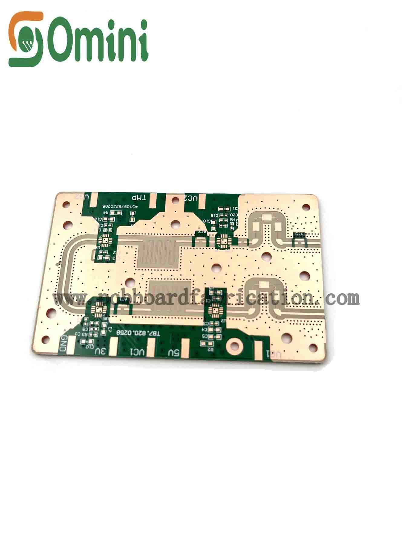
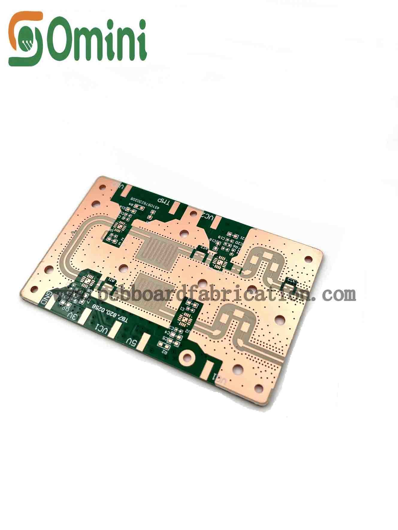
6 Layers High Speed HDI PCB ENIG For Mobile Phones And Tablets

| Place of Origin | China |
|---|---|
| Brand Name | OminiPCB |
| Certification | ISO9001, UL, TS16949 |
| Model Number | 00003 |
| Minimum Order Quantity | Negotiate |
| Packaging Details | Vacuum packing |
| Delivery Time | 3-8 work days |
| Payment Terms | L/C, T/T, Western Union, MoneyGram |
| Supply Ability | 9,999,999 |

Contact me for free samples and coupons.
Whatsapp:0086 18588475571
Wechat: 0086 18588475571
Skype: sales10@aixton.com
If you have any concern, we provide 24-hour online help.
xProduct Details
| Product Name | 6 Layers PCB High-Speed HDI PCB For Mobile Phones And Tablets With ENIG | Copper Thick | 1OZ |
|---|---|---|---|
| Base Material | SY SCGA-500 | Min. Line Space | 4mil |
| Board Thickness | 2.0mm | Min. Line Wide | 4mil |
| Min. Hole Size | 6mil | Layer | 6Layer |
| Application | Electronic Equipments,Medical Devices,Automotive | ||
| High Light | High Speed HDI PCB ENIG,6 Layers High Speed HDI PCB,6 Layers PCB For Mobile Phones |
||
Product Description
Digital test Isola High Speed Printed Circuit Board For High-speed operations
Quick details:
Base Material:SY SCGA-500
Copper Thickness: 1oz
Board Thickness: 2.0mm
Min. Hole Size: 6mil
Min. Line Width: 4mil
Min. Line Spacing: 4mil
Surface Finishing: ENIG
Board Size: Customize Min:6mm*6mm Max:457mm*610mm
Product name: High Frequency PCB
Application: Electronic Equipments,Medical Devices, Automotive
Sheet thickness: 0.1mm-7mm
Maximum board width: Customize
Type: High Speed PCB
Certificate: TS16949.ISO14001.ROHS. ISO9001
Color: Green, White, Blue, Black, Red, Yellow
Package: Vacuum packing
Description of High Speed PCB Printed Circuit Board Advantages
1.Faster signal transmission: High-speed designs are necessary for transmitting signals at higher frequencies without any loss or distortion.
2.Reduced EMI and noise: The use of High-Speed PCB design techniques such as impedance control, shielding, and proper grounding helps reduce Electromagnetic Interference (EMI) and noise.
3.Design flexibility: High-speed PCBs can be designed in various shapes and sizes according to the specific requirements of the application.
4.Higher density: With High-Speed PCBs, it is possible to pack more components into a smaller space due to smaller track widths and tighter component placement.
| Application | Use Frequency |
| Cellular & Pager Telecom | 1-3 GHz |
| GPS | 1.57/1.22GHz |
| Cars, individuals receive satellite | 2.4 GHz |
| Low noise block downconverter (LNB/LNA) | 2-3GHz |
| Direct broadcast satellite (DBS) system | 13 GHz |
| Families receiving satellite | 12-14 GHz |
| Wireless carry communication antenna system | 14 GHz |
| Very small aperture terminal (VSAT) | 12-14 GHz |
| Individuals receive base stations, or satellite launch | 13-24GHz |
| Digital microwave system | 10-38 GHz |
| Car Avoidance system (CA), | 75 GHz |
Specification Of Omini High Speed PCB Printed Circuit Board
| Layer | 2-24 layer |
| Material | Rogers: 4350B, 5880, 4003C, SY SCGA-500, S7136, Arion, Taconic |
| Board thickness | 0.4mm-5.0mm |
| Max.finished board side | 457mm*610mm |
| Min.drilled hole size | 0.25mm |
| Min.line width | 0.075mm(3mil) |
| Min.line spaceing | 0.075mm(3mil) |
| Surface finish/treatment | Electroless/immersion gold/ENIG/Immersion silver/Organic solderability |
| Copper thickness | 0.5 oz - 2.0oz |
| Solder mask color | green/black/white/red/blue/yellow |
| Inner packing | Vacuum packing, Plastic bag |
| Outer packing | Standard carton packing |
| Hole tolerance | PTH:±0.076, NTPH:±0.05 |
| Certificate | UL, ISO9001, ISO14001, RoHS, CQC |
| Profiling Punching | Routing, V-CUT, Beveling |
| Assembly Service | Providing OEM service to all sorts of printed circuit board assembly |
![]()
![]()
![]()
![]()
![]()
FAQ:
Q1:Does Omini have enough capacity to produce high-quality products?
A: Omini has 20 years of history in manufacturing PCB, more than 200 employees and 10,000㎡ factory area.We got the UL, ISO9001 certificates, and our production is sold abroad. We have engouh machines & equipment to ensure the quality, please check our Production Equipment list picturers.
Q2:How long does customers need to wait for the quotation and lead time?
A: We have a prefessional group to deal with your inquiry. In our working time, we will reply to your email within 30 minutes to show we have received your inquiry, Then we will send you our quotation in no more than 6 hours. Please noticed our working time is Monday to Friday, 8am to 24pm.
Q3:How can I make sure my PCB gerber is safety?
A: We promise we won't divulge your gerber to the 3rd party, one of our responsibilities is protecting customer information privacy and security, customer information can be included: company name, address, number, trademark, ect. And we could sign NDA with client if necessary.
Recommended Products