


All Products
-
 Tyler MartinThe quality of the PCBs I received from this company was outstanding. They were well-made and exceeded my expectations.
 -
Olivia AndersonI've been using this company for all of our company PCB needs for years and I have never been disappointed. Their products are always consistent and reliable, and their prices are very competitive.
-
Ashley Williamswell-packaged and arrived in perfect condition. I would definitely recommend them to anyone in need of high-quality PCBs
Contact Person :
Xu
Phone Number :
0086 18565798250
Whatsapp :
+008618576405228
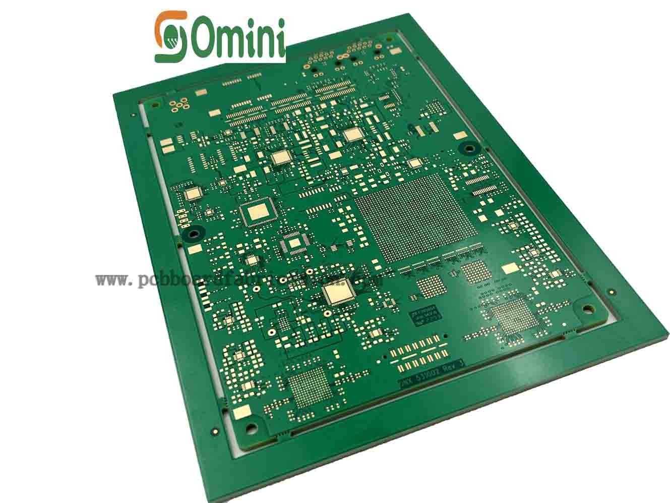
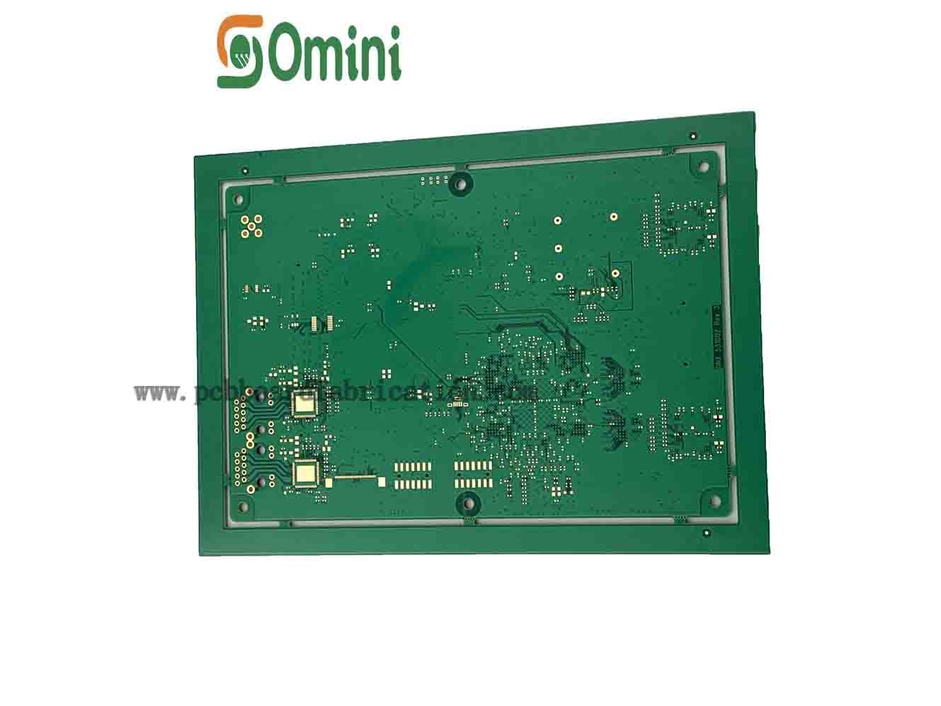
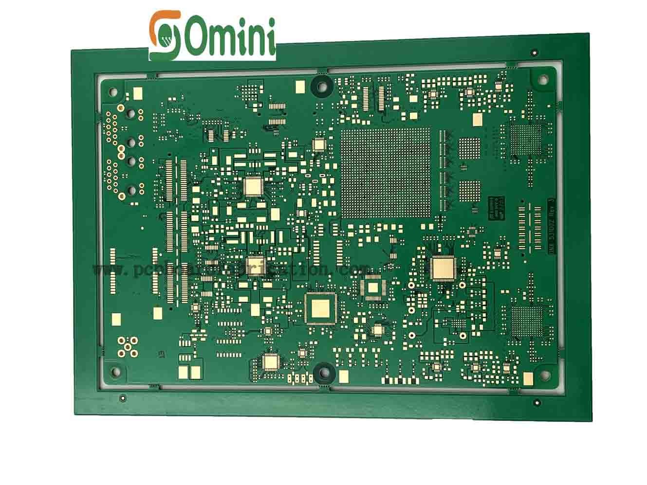
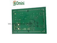
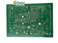
2 Layer Double Sided PCB With Via In Pad For Miniaturized Devices
| Place of Origin | China |
|---|---|
| Brand Name | OminiPCB |
| Certification | ISO9001, UL, TS16949 |
| Model Number | 0601 |
| Minimum Order Quantity | Negotiate |
| Price | Negotiate |
| Packaging Details | Vacuum packing |
| Delivery Time | 3-8 work days |
| Payment Terms | L/C, T/T, Western Union, MoneyGram |
| Supply Ability | 9,999,999 |

Contact me for free samples and coupons.
Whatsapp:0086 18588475571
Wechat: 0086 18588475571
Skype: sales10@aixton.com
If you have any concern, we provide 24-hour online help.
xProduct Details
| Product Name | Double-sided PCB | Base Material | FR4 |
|---|---|---|---|
| Copper Thick | 1 OZ | Min. Line Space | 6 Mil |
| Board Thickness | 1.6 Mm | Min. Line Wide | 6 Mil |
| Min. Hole Size | 12 Mil | Layer | 2 Layers |
| Application | Industrial Control, Communications, Household Appliances, Automotive Electronics | ||
| High Light | Double Sided PCB For Miniaturized Devices,Via In Pad Double Sided PCB,Via In Pad 2 Layer PCB |
||
Product Description
Double Sided Layer PCB with Via-in-Pad for Miniaturized Devices
Quick details:
Base Material: FR4
Copper Thickness: 1 oz
Board Thickness: 1.6 mm
Min. Hole Size: 12 mil
Min. Line Width: 6 mil
Min. Line Spacing: 6 mil
Surface Finishing: OSP/Gold Finger/LFHASL/ENIG/ENEPIG
Board Size: Customize
Product name: Double Sided Layer PCB with Gold Plating for High-Reliability Applications
Material: Rogers, Taconic, Arlon, Nelco
Application: Industrial Control, Communications, Household Appliances, Automotive Electronics
Sheet thickness: 0.1MM-7MM
Maximum board width: Customize
Type: Double-sided PCB
Certificate: ISO9001,
Color: Customize
Package: Vacuum packing or anti-static packing (included humidity card and desiccant)
Description of Different Types of Via-in-Pad Printed Circuit Board:
1.The most common plate hole
It means that the via hole is punched on the pad, and no special process is required to make the PCB. There will be a "hole" on the pad. If the hole is too large, it may cause tin leakage or false soldering. This process The cheapest and most common are the thermal vias on the QFN package below.
2.Resin plug hole + electroplated copper cap
The hole process of this type of plate is a bit more complicated. First, fill the hole with epoxy resin, and then electroplate copper to seal it. There is no hole in the hole on the surface. It is very smooth, and there will be no tin leakage or soldering problems. The process is generally used on relatively high-end HDI boards. For example, high-precision devices are used on the board, such as BGA and other devices with multiple pins. The pin spacing is too small to fan out. This kind of hole in the plate has a great advantage, making the wiring smooth. Compared with the ordinary hole-in-disk process, it is relatively complicated, and of course the cost will also increase. Now the mobile phone board is designed with a hole in the plate.
3.Copper paste plug hole + electroplated copper cap
This type of hole-in-disc technology is generally used in positions that require fast heat conduction, such as the GND PAD under QFN. The middle of the via hole is filled with copper paste, and then sealed with electric copper. Since the center of the via hole is filled with copper metal, the thermal conductivity is very good, and it is no different from the resin plug hole from the surface.
Specification of Omini Double-sided PCB Printed Circuit Board:
| 1 | Layer | 2 Layers |
| 2 | Material | Rogers, Polymide, Arlon, Nelco, Taconic |
| 3 | Board thickness | 0.4mm - 5.0mm |
| 4 | Max.finished board side | 457mm*610mm |
| 5 | Min.drilled hole size | 0.25mm |
| 6 | Min.line width | 0.075mm(3mil) |
| 7 | Min.line spaceing | 0.075mm(3mil) |
| 8 | Surface finish/treatment |
Electroless nickel/immersion gold (ENIG) - RoHS Immersion tin - RoHs Immersion silver - RoHS Organic soldersbility preservatives - RoHs |
| 9 | Copper thickness | 0.5 OZ- 2 OZ |
| 10 | Solder mask color | green/black/white/red/blue/yellow |
| 11 | Inner packing | Vacuum packing, Plastic bag |
| 12 | Outer packing | Standard carton packing |
| 13 | Hole tolerance | PTH:±0.076, NTPH:±0.05 |
| 14 | Certificate | UL, ISO9001, ISO14001, ROHS, CQC |
| 15 | Profiling Punching | Routing, V-CUT, Beveling |
| 16 | Assembly Service | Providing OEM service to all sorts of printed circuit board assembly |
![]()
![]()
![]()
![]()
![]()
FAQ:
Q1:Does Omini have enough capacity to prodece high-quality products?
A: Omini has 20 years of history in manufacturing PCB, more than 200 employees and 10,000㎡ factory area.We got the UL, ISO9001 certificates, and our production is sold abroad. We have engouh machines & equipment to ensure the quality, please check our Production Equipment list picturers.
Q2:How long does customers need to wait for the quotation and lead time?
A: We have a prefessional group to deal with your inquiry. In our working time, we will reply to your email within 30 minutes to show we have received your inquiry, Then we will send you our quotation in no more than 6 hours. Please noticed our working time is Monday to Friday, 8am to 24pm.
Q3:How can I make sure my PCB gerber is safety?
A: We promise we won't divulge your gerber to the 3rd party, one of our responsibilities is protecting customer information privacy and security, customer information can be included: company name, address, number, trademark, ect. And we could sign NDA with client if necessary.
Recommended Products