


All Products
-
 Tyler MartinThe quality of the PCBs I received from this company was outstanding. They were well-made and exceeded my expectations.
 -
Olivia AndersonI've been using this company for all of our company PCB needs for years and I have never been disappointed. Their products are always consistent and reliable, and their prices are very competitive.
-
Ashley Williamswell-packaged and arrived in perfect condition. I would definitely recommend them to anyone in need of high-quality PCBs
Contact Person :
Xu
Phone Number :
0086 18565798250
Whatsapp :
+008618576405228
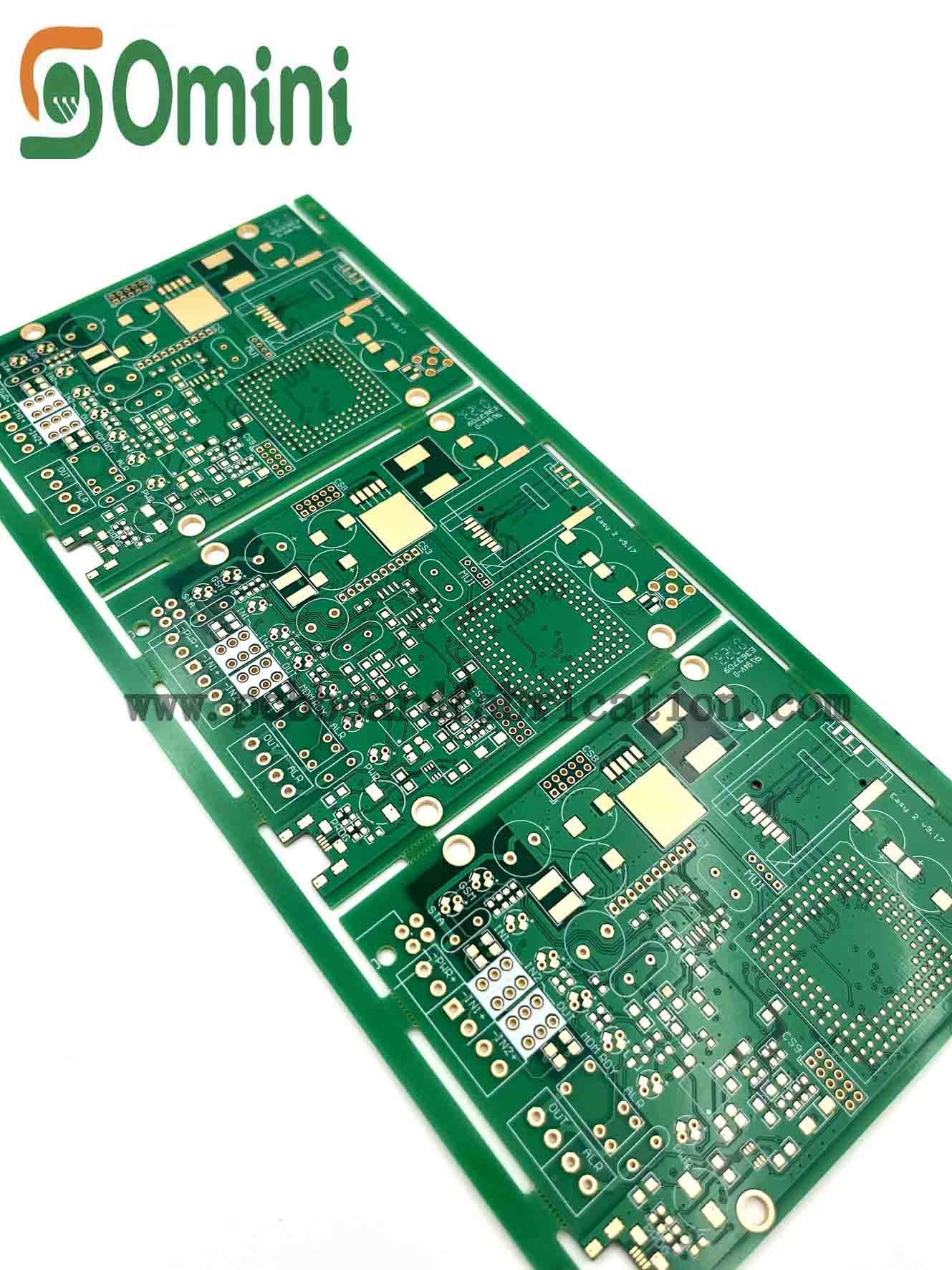
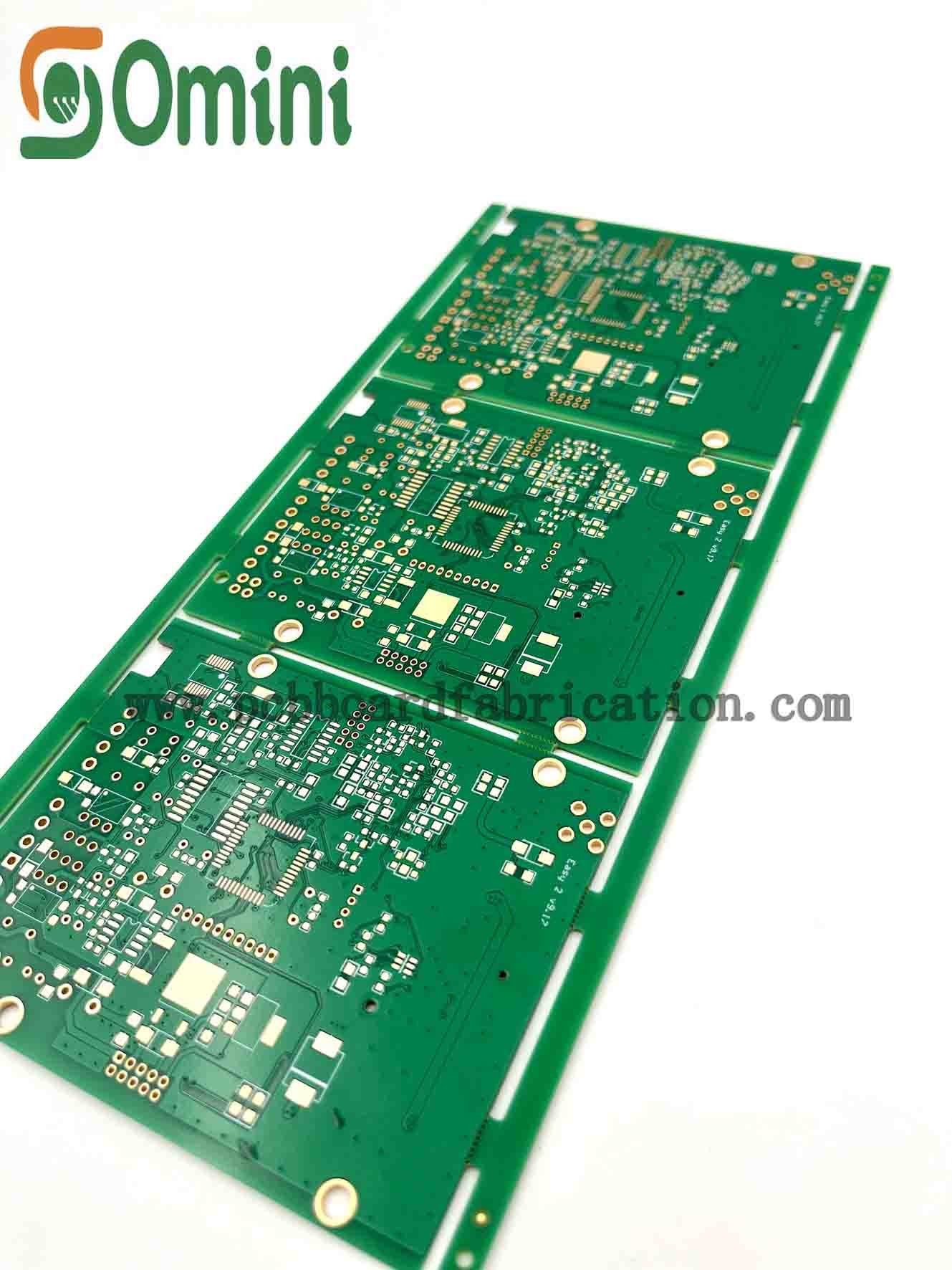
High Density Interconnect Double Sided PCB With Blind Buried Vias
| Place of Origin | China |
|---|---|
| Brand Name | OminiPCB |
| Certification | ISO9001, UL, TS16949 |
| Model Number | 0601 |
| Minimum Order Quantity | Negotiate |
| Price | Negotiate |
| Packaging Details | Vacuum packing |
| Delivery Time | 3-8 work days |
| Payment Terms | L/C, T/T, Western Union, MoneyGram |
| Supply Ability | 9,999,999 |

Contact me for free samples and coupons.
Whatsapp:0086 18588475571
Wechat: 0086 18588475571
Skype: sales10@aixton.com
If you have any concern, we provide 24-hour online help.
xProduct Details
| Product Name | Double Sided Layer PCB With Blind/Buried Vias For High-Density Interconnect Applications | Base Material | FR4 |
|---|---|---|---|
| Copper Thick | 1 OZ | Min. Line Space | 4mil |
| Board Thickness | 1.6 Mm | Min. Line Wide | 4mil |
| Min. Hole Size | 6mil | Layer | 2 Layers |
| Application | LED Lighting, Printers, HVAC, Converters | ||
| High Light | High Density Interconnect Double Sided PCB,high density interconnect pcb,Blind Buried Vias Double Sided PCB |
||
Product Description
Double Sided Layer PCB with Blind/Buried Vias for High-Density Interconnect Applications
Quick details:
Base Material: FR4
Copper Thickness: 1 oz
Board Thickness: 1.6 MM
Min. Hole Size: 0.15MM(Mechanical),0.1MM(HDI)
Min. Line Width: 0.075MM
Min. Line Spacing: 0.075MM 3mil/4mil
Surface Finishing: OSP/Gold Finger/LFHASL/ENIG/ENEPIG
Board Size: Customize
Product name: High Frequency PCB
Material: Rogers, Taconic, Arlon, Nelco
Application: Telecommunications, Military and aerospace, Automotive, High-density interconnect
Sheet thickness: 0.1MM-7MM
Maximum board width: Customize
Type: High Frequency PCB
Certificate: ISO9001,
Color: Customize
Package: Vacuum packing or anti-static packing (included humidity card and desiccant)
Description Of Double-sided PCB Printed Circuit Board
Double Sided Layer PCB with Blind/Buried Vias is a highly advanced technology that enables the design of high-density interconnects for compact and miniature electronic devices. This technology allows for the creation of intricate circuitry with components mounted on both sides of the PCB, while still maintaining a low profile and small form factor.
Blind vias and buried vias are drilled into the PCB layers to allow for the routing of signal traces between layers without impacting the outer layers. This technique reduces the amount of surface area required for routing and allows for higher component densities on the PCB. This means that more components can be placed on the same size board, allowing for more functionality in a smaller space.
Double Sided Layer PCB with Blind/Buried Vias are widely used in applications such as smartphones, tablets, wearable devices, and other portable electronic devices. These PCBs are also used in high-speed networking equipment, aerospace, and military applications.
The design of these PCBs requires precision and expertise, as the placement and routing of the vias must be optimized to ensure the highest possible performance. With the use of advanced software and manufacturing techniques, Double Sided Layer PCB with Blind/Buried Vias can be manufactured with a high degree of accuracy and reliability.
Overall, Double Sided Layer PCB with Blind/Buried Vias is an essential technology for the creation of compact and high-density electronic devices with complex circuitry. It allows for the creation of smaller and more powerful devices, making it a vital component in the advancement of technology.
Specification of Omini Double-sided PCB Printed Circuit Board
| 1 | Layer | 2 Layers |
| 2 | Material | Rogers, Polymide, Arlon, Nelco, Taconic |
| 3 | Board thickness | 0.4mm - 5.0mm |
| 4 | Max.finished board side | 457mm*610mm |
| 5 | Min.drilled hole size | 0.25mm |
| 6 | Min.line width | 0.075mm(3mil) |
| 7 | Min.line spaceing | 0.075mm(3mil) |
| 8 | Surface finish/treatment |
Electroless nickel/immersion gold (ENIG) - RoHS Immersion tin - RoHs Immersion silver - RoHS Organic soldersbility preservatives - RoHs |
| 9 | Copper thickness | 0.5 OZ- 2 OZ |
| 10 | Solder mask color | green/black/white/red/blue/yellow |
| 11 | Inner packing | Vacuum packing, Plastic bag |
| 12 | Outer packing | Standard carton packing |
| 13 | Hole tolerance | PTH:±0.076, NTPH:±0.05 |
| 14 | Certificate | UL, ISO9001, ISO14001, ROHS, CQC |
| 15 | Profiling Punching | Routing, V-CUT, Beveling |
| 16 | Assembly Service | Providing OEM service to all sorts of printed circuit board assembly |
![]()
![]()
![]()
![]()
![]()
FAQ:
Q1:Does Omini have enough capacity to prodece high-quality products?
A: Omini has 20 years of history in manufacturing PCB, more than 200 employees and 10,000㎡ factory area.We got the UL, ISO9001 certificates, and our production is sold abroad. We have engouh machines & equipment to ensure the quality, please check our Production Equipment list picturers.
Q2:How long does customers need to wait for the quotation and lead time?
A: We have a prefessional group to deal with your inquiry. In our working time, we will reply to your email within 30 minutes to show we have received your inquiry, Then we will send you our quotation in no more than 6 hours. Please noticed our working time is Monday to Friday, 8am to 24pm.
Q3:How can I make sure my PCB gerber is safety?
A: We promise we won't divulge your gerber to the 3rd party, one of our responsibilities is protecting customer information privacy and security, customer information can be included: company name, address, number, trademark, ect. And we could sign NDA with client if necessary.
Recommended Products